Operationnal Amplifiers
(Last update November. 4 2009, Update May 12 2017)
Operational amplifiers
are
used in wide variety in integrated circuit design. The variety of
topologies
results from different application requirements such as:
-
high
accuracy
(also see autozero
OPs too)
- low
noise
- low
current consumption
- high
speed
- input
common mode range (rail to rail)
-
output
voltage swing
-
output
impedance
-
response
to input overdrive
- input
impedance
- low
cost
- Instrumentation
Amplifiers
Some of these design
targets
exclude one another or only can be achieved together at very high
effort.
This leads to a big variety of topologies.
The Circuits
Since the variety of
topologies
is so big this page will NEVER be complete. I simply add circuits as I
need them for trainings.
The Basics
Opamps can be sorted by the number of gain stages. Today (2008) most
common designs use 2 stages or in some cases 3 stages. Since the
voltage gain drops with technologies using shorter channel length low
voltage designs may even require higher numbers of stages in the future.
Single Gain Stage Amplifier
This is the most generic operational amplifier. It consists of a
differential amplifier and a unity gain voltage follower. Usually the
gain is low but it is very nice for learning how it works. So here it
is kept as a tutorial example.
The load of the differential amplifier can be a resistor or - more
frequently found - a current mirror.
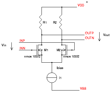
Fig. 1: Example of a Differential Stage with Resistor Load
Normally R1 and R2 are equal. So in the following we assume:
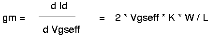
So the differential voltage gain becomes:
gm is the transconductance of the MOS transistors. gm depends on
technology (mainly gate oxide thickness tox), temperature (carrier
mobility is a function of temperature), transistor width W, transistor
length L, and bias current Ibias. Technology parameters usually are
hidden in the factor K.
In strong inversion the current of a MOS transistor calculates as:
Since we need gm of one of the transistors of the differential
ampliifer we have to derive this equation:
So what is Vgseff ?
Id in the balanced operating point is half of Ibias. So it can be
calculated.
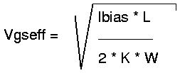
Plugging this expression into the equation of gm of one of the
transistors we get:
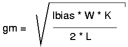
Thus the voltage gain becomes:
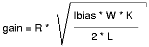
(Remark: One transistor only 'sees' half of the change of Vin but at
the output Vout is differential again so we see both hafts again.)
To get a rough idea of the performance of such an amplifier let us use
some numbers:
K = 50 uA/V2, L=2um, W=100um,
Ibias=100uA, R=100K
gain = 11.18
To increase the gain of the single stage amplifier with resistor load
the following can be done:
- maximize R
- maximize W/L
- maximize Ibias
Changing Ibias or R changes the DC operating points and the required
supply voltage VDD. Replacing the resistors by an active load is much
more elegant.
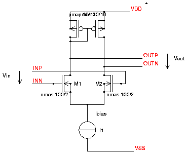
Fig. 2: Example of a Differential Amplifier with Active Load
Now node OUTN has become a current summing point with different signs
for M1 and M2. Any increase of the current of M1 pulls up node OUTN. An
increase of the current through M2 pulls down node OUTN. Besides
that the impedance oa node OUTN is very high now because M2 as well as
the PMOS transistor act as current source and current sink.
So what is the output resistance of OUTN? It now is defined by the
early voltage of the shortest transistor accessing the node and the
current flowing through the transistor. (to be precise: both transistor
output impedances are parallel. But since the current mirror transistor
usually is factors longer than the differential amplifier transistor M2
we neglect it here.)

The early voltage is roughly proportional to the length of a transistor
with about Kearly = 10V/um.
Neglecting the long PMOS transistors all the performance still depends
on the differential stage transistors.
So the voltage gain in strong inversion becomes
Using the same transistor parameters as before and using Kearly =
10V/um we end up with a gain of about 141 or 46dB.
To improve the gain the following can be done:
- increase L
- increase W
- reduce the bias cirrent Ibias until we reach the edge of weak
inversion (here the equations change!)
Increasing W, L and reducing the bias current however makes the
amplifier slow!
This simple one gain stage amplifier still is used in voltage
regulators. The following figure shows the regulator amplifier of the
MC1723L (taken from Motorola, Linear Integrated Circuit Data Book, 1971)
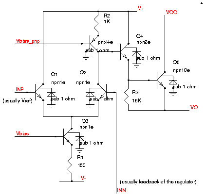
Fig. 3: Example of an actual implementation of a single gain stage
OPAMP (MC723L)
Having only one gain stage the frequency compensation is fairly fool
proof. This is the main reason for still using this circuit. Besides
that bipolar transistors offer higher gm and better early voltages
(arround 40..100V). So in bipolar technologies the single stage
amplifier can be designed to reach a voltage gain of up to about 60dB.
The first publication of such a differential amplifier I am aware of
dates back to 1938:
J.F. Toennies, "A Differential Amplifier", Review of Scientific
Instruments, Vol. 9, March, 1938, pp 95-97.
Refinements of Single Stage Differential Amplifiers
There are several possibilities of refining the circuit to achieve
higher gains at the cost of higher supply voltage or higher current
consumption:
- Operation in weak inversion
- Telescopic amplifiers (traditional cascodes)
- Folded cascodes
Two Stage Operational Amplifiers
Today using two gain stages is the most common approach of designing
operational amplifiers. The first (differential) stage is used as an
operational transconductance amplifier (OTA) driving a second gain
stage. This way the gains of both stages multiply.
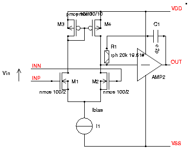
Fig. 4: Two Stage OPAMP
Since we have two gain stages now we have to take care about
stability. Without C1 each stage at a certain frequency starts to
act ans an integrator. So the phase shift would approach 2*90°.
Feeding the signal back to the inverting input to define the closed
loop gain would lead to oscillation. So there must be one dominant pole
provided by the capacitor C1.
Typical examples of the two stage approach are:
ADI model 121 (Analog Devices, 1966)
LM101 (National Semiconductor, 1968)
uA741 (Fairchild, 1968)
CMOS implementations like ICL7611 of Intersil were introduced a bit
later arround 1976.
The most basic bipolar
amplifier
This topology dates back
to
the 1960's. Probably the most simple and cheapest possible.
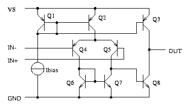
Fig. 5: The most comon
bipolar
opamp
Limitations of this
topology
are:
-
common
mode range 200mV to VS-0.9V
- PNPs
are slow
-
output
current capability only some uA
- input
bias current of Q4, Q5
- only
medium gain
- not
compatible with CMOS technology
The most simple CMOS
opamp
Converting the bipolar
circuit
into a CMOS design is easy. The circuit is in use since the beginning
of the
1970's.
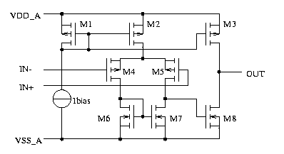
Fig. 6: simple CMOS opamp
We improved the
following
parameters:
-
faster
because small MOS transistors have less capacities.
- no
more input bias current.
- CMOS
technology compatible
But we sacrificed other
parameters
compared to the previous bipolar version:
-
common
mode range 200mV to VDD_A-1.5V (assuming about 0.8V threshold)
- gate
break down limit input voltage range
- lower
gain than bipolar version
-
higher
offset (unless extreme sizes are used)
- more
noise
Norton amplifier
To allow higher input
voltages
and a wider common mode range the norton amplifier topology can be
used.
Bipolar counter parts exist since the 1970's (LM159, LM369)
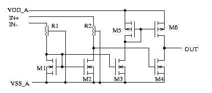
Fig. 7: norton amplifier
Now the input
transistors
are replaced by R1 and R2. M1 and M2 simply compare the currents
flowing
through R1 and R2. M4's threshold must matchthe thresholds of M1 and
M2.
To operate M4 at exactly the same operating point M3, M5, M6 provide
exactly
the same operating point. Accuracy (offset) mainly depends on the
matching
of R1 and R2.
Advantages:
- very
cheap
- input
voltage is only limited by the rupture of R1, R2
Drawbacks:
-very
poor offsets (example R1, R2 matching 0.3%, Vin versus VSS_A is 5V
-> 15mV
offset)
- early
voltages of M3, M4, M6 further increase offsets
- high
input bias current
3 Gain Stage Topologies
Reducing the channel length and the supply voltage the gain of the
amplifier gets lower and lower. To overcome this problem the number of
gain stages is further increased mainly in low voltage designs.
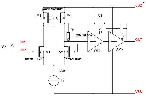
Fig. 8: Concept of an OPAMP with three gain stages
The new stage is the non inverting amplifier between the
differential stage and the output stage. To keep the feedback
capacitors in an affordable range (some pF) this non inverting stage
usually is implemented an an OTA.
First implementations of 3 stage amplifiers are very old:
uM709 (Fairchild, 1965) is already a 3 stage
design!
The concept was not estimated too much because frequency compensation
of the 709 was cumbersome. But low supply voltage and short channel
transistors lead to a renaissance of 3 stage amplifiers in the 1980s.
LH0062 (National Semiconductor, 1976, used
already nested miller compensation!)
Huijsing, JSSC Dec. 1985, pp1144-1150 (uses
nested miller compensation)
OP-05 (Linear Technology, 1990, uses individual
comp. of each stage)
LT1001 (Linear Technology, 1990, nested miller
compensation)