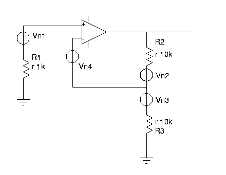
Operational amplifiers
usually are operated in a closed loop
Fig. 1 Operational
amplifier in a typical application
Let us assume a
real amplifier consists of a noisless ideal amplifier and an input
noise source Vn4. Besides that the application circuit holds 3 more
noise sources:
Vn1: the noise of resistor R1. (Usually R1 is the impedance of the
signal source connected to the input of the amplifier).
Vn2: the noise of resistor R2.
Vn3: the noise of resistor R3.
Each of these noise signals propagates to the output of the amplifier
with a certain gain ngx.
Propagation of Vn1:
ng1 = Vn1out /
Vn1 = (R1+R3)/R3
(1)
Propagation
of Vn2:
Since the ideal
operational amplifier always regulates the differetial voltage to 0V
the foot of Vn2 is
at 0V (vitual ground). Therefore Vn2 = Vn2out
ng2 =
1
(2)
Propagation of Vn3:
R3 is grounded
on one
side. The otherside is nulled by the amplifier. Thus Vn3 creates a
current of
I3=-Vn3 /
R3
(3)
Since the ideal
operational amplifier has an infinite input impedance the only
available path for I3 is
through R2. Therefore the output voltage of the amplifier becomes:
Vn3out = I3 * R2
= -Vn3 * R2 / R3
(4)
ng3 = R2 / R3
(5)
Propagation of Vn4:
The input of the
amplifier is nulled. The feedback reproduces the voltage -Vn4 across
R3. The current flows through R2 and R3 creating an output voltage of:
Vn4out = -Vn4 *
(R2+R3) / R3
(6)
Thus the noise
gain for Vn4 is:
ng4 = -(R2+R3) /
R3
(7)
Adding the contributions:
All noise
sources are
assumed uncorrelated. The powers of the amplified noise sources add.
Vnout2
=
(ng1*Vn1)2 + (ng2*Vn2)2 + (ng3*Vn3)2 +
(ng4*Vn4)2
(8)
Calculation
of the
contributions Vn1 to Vn3:
To solve this
equation the noise voltages Vn1 to Vn4 are needed.
Vn1 to Vn3 are resistive noise sources. Assuming resistors without
junctions inside (This applies to many, but not necessarily to all
resistive materials) the thermal noise voltage calculates:
Vnx =
SQRT(4*k*T*R*df)
(9)
with:
k = Boltzmann constant = 1.38*10-23J
T = Temperature in Kelvin
R = resistance in Ohm
df = Bandwidth considered in Hz
Calculation
of the
Amplifier Noise Vn4:
Calculation of
the amplifier noise requires knowing the input stage of the amplifier.
Usually this is a parameter provided by the amplifier manufacturer.
If the input stage is known the noise can be calculated except for very
low frequencies. At very low frequencies (usually below 10kHz) the 1/f
noise may dominate thermal noise and shot noise. 1/f noise has many
different sources mainly related to carrier generation and
recombination. 1/f noise estimation requires technolology data that
often is measured empirically. Therefore in
the following 1/f noise is not considered. So the following applies to
frequencies
above roughly 3kHz to 10kHz excluding 1/f noise.
The following
figure
shows a MOS differetial stage including noise sources.
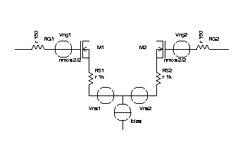
Fig. 2: Differential input
stage
with noise sources
The two
resistors
in the gate path are wire resistances and gate polysilicon resistances.
(The
impedance of the signal source is already treated in figure 1). For low
noise
amplifiers using a low resistive gate and many contacts in parallel is
recommended.
(In the example shown above these resistors RG1 and RG2 are 150 Ohm
each.
This leads to a resistive single ended input noise of about
1.6nV/SQRT(Hz)
at room temperature)
RS1 and RS2 are the source impedances. Normally there are no
intentional
resistors at this location (unless you want to reduce the gain). So RS1
and
RS2 are the inverse of the transconductance.
RG1 = RG2 = 1/gm
(10)
Since gm
increases
with the square root of the bias current:
gm = 2*SQRT(k*Id * W /L)
(11)
the resistive
noise
can be reduced increasing the bias current and W/L. Choosing a
technology
with thin gate oxide leading to a higher k and using NMOS transistors
rather
than PMOS transistors for the input stage is a good idea too.
(As an example let us assume we use a 15nm gate oxide. As a rule of
thumb
we can expect k in the range of 2000uA/V2 *nm / tox for nmos
transistors.
with W/L=10 and a bis current of 50uA (25uA in each transistor) we end
up
with about
gm=600uA/V or RS1 = RS2 = 1.4K
So the single
eded
resistive noise in the source is about 5nV/SQRT(Hz). )
Additionally to
the
resistive noise each electron passing through the channel causes a
'granularity'
of the current. This quantisation of the current produces the so called
shot
noise.
Ishot_noise = SQRT(2*e*I*df)
(12)
with e being the
electron
charge of 1.602*10-19As
since all other
noise
sources are refered to a bandwidth of 1 Hz it is conveniant to do the
same
here.
Ishot_noiseHz = SQRT(2*e*I)
(13)
This shot noise
current
leads to a further noise signal at the resistances RS1 and RS2 (1/gm
respecively).
(Returning tho our example with I=25uA the noise current becomes
Ishot_noiseHz = 2.83pA/SQRT(Hz)
This current
causes
a drop of 3.9nV/SQRT(Hz) over R1 and R2.)
The total noise
voltage
is the square root of the summ of the squares of all noise sources.
Since
we are dealing with a differential stage each source exists twice (one
on
each side of the amplifier)
Vnoise = SQRT(4*k*T*RG1*df + 4*k*T*RG2*df + 4*k*T*df /gm + 4*k*T*df /gm + 4*k*T*df /gm + 2*e*I*df/gm + 2*e*I*df/gm)
(In our example
we
end up with:
VnoiseHz = SQRT(2.56nV2 + 2.56nV2+ 25nV2+ 25nV2+ 15.2nV2+ 15.2nV2) / SQRT(Hz)
VnoiseHz= 9.24nV/SQRT(Hz)
Assuming we had
to
build a linear amplifier with a bandwidth of 20kHz the in band noise
would
be 1.3uV.)
Bipolar
amplifiers
follow the same calculation except that in stead of noise in the gate
resistance
we have to consider the noise of the base resistance and 1/gm will be
replaced
by k*T/e .
In practical design the noise performance of (vertical!) bipolar
transistors
often is better because surface elements (MOS as well as lateral PNPs
often
suffer from surface states increasing generation and
recombination.
The higher generation and recombination rate due to surface states and
contamination
in lateral
transistors
leads to a
higher
1/f noise.