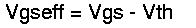
CMOS Input Stages
(Last update Nov. 25 2005, Update May 12 2017)
Usually the
parameter of highest interrest is the offset of an operational
amplifier.
There are many
possible causes of offset such as layout assymetries, temperature
gradients, process inhomogenities etc. Assuming the design is done by
an experienced designer and the process is well under control the
systematic errors are assumed to be negligible in the following
calculations. Thus the remaining errors are of statistical nature. They
result from statistical spread of properties such as gate oxide
thickness, random distribution of dopants in the transistors, gate
length and gate width deviations etc.
The most
important parameter describing MOS transistor matching is the
technology specific offset "Vostech" typically given in mV*um.
As a rule of
thumb for reasonably large transistors we can assume:
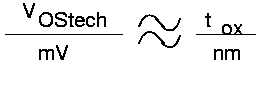
The unit of VOStech is mVum
The offset of
transistors (one sigma) calculates as:
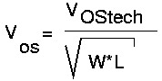
example:
tox = 20nm,
Vostech=20mVum, W=20um, L=2um
Vos =
20mV/SQRT(40) = 3.16mV
Typical values
published in IEEE journal of solid state circuits 1994 by Francesco
Forti and Michael E. Wright are:
tox
|
technology
|
gate area um2
|
Vos/mV
|
Vostech/mV
|
20nm
|
M/HP
|
3000
|
0.3
|
16
|
20nm
|
M/HP
|
150
|
1.2
|
14.7
|
20nm
|
M/HP
|
3
|
20
|
34.6
|
40nm
|
M/Orbit
|
8000
|
0.7
|
62.6
|
40nm
|
M/Orbit
|
2000
|
1.5
|
67.1
|
40nm
|
M/Orbit
|
70
|
4.0
|
33.5
|
20nm
|
UTMC
|
100
|
2.0
|
20
|
20nm
|
UTMC
|
18
|
3
|
12.7
|
20nm
|
IBM
|
300
|
8
|
138
|
20nm
|
IBM
|
400
|
6
|
120
|
The table shows
that this more ore less empirical rule of thumb applies to many, but
not necessarily to all technologies!
Typical MOS operational amplifiers consist of a differential pair and a
current mirror.
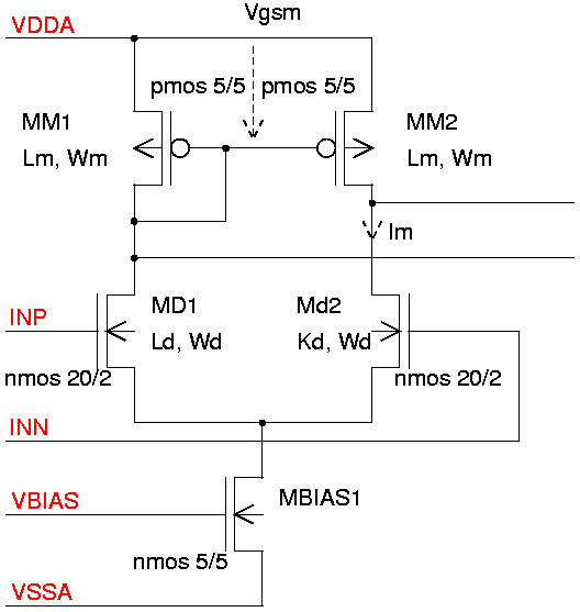
Fig. 1: Input stage of a simple operational amplifier
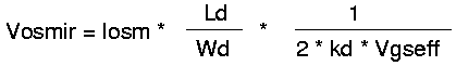
The current mirror can significantly contribute to the
offset of the amplifier. To get an idea of the error propgation the
voltage offset of the current mirror must be converted into a current
offset. Assuming the current mirror transistors operate at low current
densities but not in subthreshold regime the current of a transistor in
the mirror is:
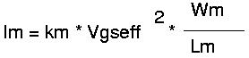
with
The derivative becomes:
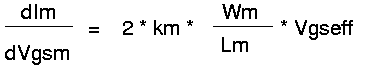
an offset voltage Vosm changes the current by:
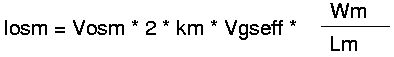
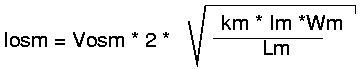
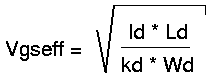
replacing Vgseff by the drain current Im this converts into:
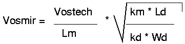
Through the differential stage the current error of the mirror
propagates to the input of the amplifier as an offset voltage. With km
being the transcondurctance of the mirror and kd being the
transconductance of the differential stage the resulting additional
offset Vosmir becomes:
with Vgseff being the effective gate voltage of the differential
amplifier transistors now.
Replacing Vgseff as before by:
we find:
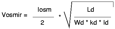
Vosm = SQRT((Wm*Ld*km)/(Lm*Wd*kd)) * dVgs
In the
following we assume no current is taken out of the differential stage
and Id = Im.
(This for instance does not apply to
folded cascodes! There you pay the better supply rejection and AC
performance with an offset penalty!)
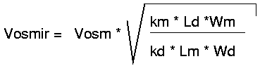
Replacing Vosm we end up with:
Assuming the offset of the current mirror and the offset of the
differential stage are statistically independent the total offset
calculates as:
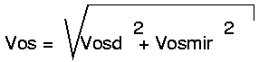
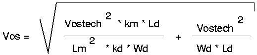
Assuming that the matching property Vostech is equal for both, NMOS and
PMOS (it should at least be similar as long as the same gate oxide is
used) the above equation becomes:
The simple case described here is available as a spread sheet for EXEL
5.0: offset.xls
In case different gate oxides are used for NMOS and PMOS the left
Vostech is the property of the PMOS transistors while the right Vostech
is the property of the NMOS transistors of our example circuit.
In this equation Wm and Lm are the width and length of the mirror
transistors.
Wd and Ld are width and length of the differential amplifier transistors
km describes the characteristic of the mirror trnansistors.
kd describes the characteristic of the differential stage transistors.
km and kd are inverse proportional to the gate oxide thickness. Due to
the different carrier mobilities of a PMOS and an NMOS transistor k of
an NMOS transistor usually is between factor 2 and factor 3 bigger than
k of a PMOS transistor. Typical values at room temperature are:
Gate oxide
|
k of NMOS
|
k of PMOS
|
10nm
|
200uA/V2 |
80uA/V2 |
20nm
|
100uA/V2
|
40uA/V2
|
40nm
|
50uA/V2 |
17uA/V2 |
Conclusion:
Usually the parameters of the input pair are most important for the
offset. The propagation of the current mirror errors can be minimized
making the mirror transistors as long as possible (at least as long as
the gate voltage requirements of the mirror transistors can be
satisfied) and making the input
transistors as wide as possible. Choosing NMOS transistors for the
differential stage (high kd) and PMOS transistors for the mirror (low
km) this further improves accuracy compared to the inverse
polarity using te same total transistor area.
Care must be taken that the transistors of the differential stage are
not too short. Extremely short transistors will suffer from hot carrier
degradation. Don't choose shorter channels than
Lmin (in um) = Vds (in V) / 2
unless the total time of operatin is only in the range of seconds
(EEPROM write amplifiers etc.) or degradation does not matter in the
specific application.