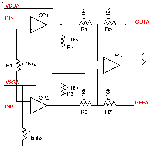
Fig. 1: Classical instrumentation amplifier
The gain of te amplifier depends on a total number of 5 resistors. 4 of them (R4, R5, R6, R7) must almost perfectly be matched to achieve a good common mode rejection!
If the number of amplifiers is to be reduced the input stage must be linearized for istance with resistors in the ifferential stage (2).
The following shows a more integration oriented topology (3). It exists as bipolar as well as CMOS implementation. One of the first implementations was the LM163 of National Semiconductors.
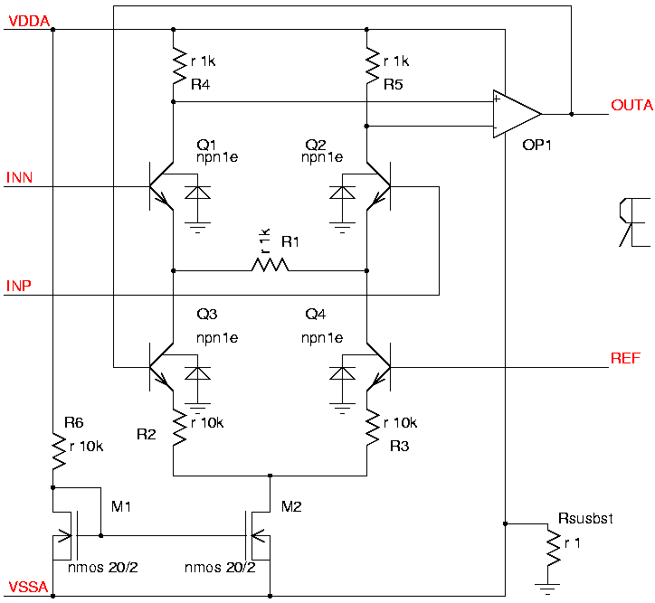
Fig. 2: Concept of the LM163 instrumentation amplifier
In this circuit the gain can be varied in a wide range adjusting R1.
Common mode rejection and offset depend mainly on the matchings R2, R3 and R4, R5 together with the bias current provided by R6, M1, M2. The amplifier OP1 contributes additionally. Depending on the common mode range desired the ratio R2/R4 = R3/R5 must be choosen. The higher this ration the higher the impact of the offset of OP1. Nevertheless usually the term
Vos1 = I(M2) * matching(R2, R3, R4, R5)
dominates the other offset sources.
Today CMOS-implementations are more frequent. Derived from the LM163 concept a CMOS implementation could look like this:
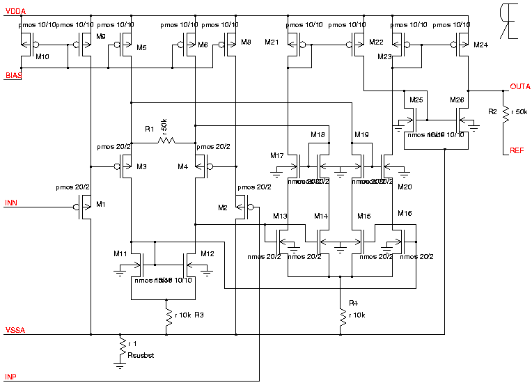
Fig. 3: CMOS instrumentation amplifier input stage
The circuit of figure 3 only needs 2 well matching resistors R1 and R2. (R3 and R4 only defne the bias current of the amplifier). The resistors R4 and R5 of the LM163 are replaced by current mirror M11 and M12. This leads to a high gain of the input stage (M3, M5) and relaxes offet requirements of the following stage (M13 to M16).
In stead o converting an output voltage back into a current (Q3, R2 of figure 2) the output current of the amplifier stage (M14, M15 of figure 3) is directly fed back to R1.
The output pin OUTA is driven by a replica of this current provided by the mirrors M21..M26 and M13, M16.
Since the output is a current source OUTA usually is followed by a unity buffer not shown above.
The offset voltage of the amplifier depends mainly on the current matching of M5 and M6, the matching of M11 and M12. Contributions of M1..M4 and M8, M9 usually are less significant.
Matchng errors of the mirrors M21..M26 directly propagate to the output. This can be regarded as an offset source as well.
To eliminate the impact of the matchings of M13 to M26 the following modification can be used:
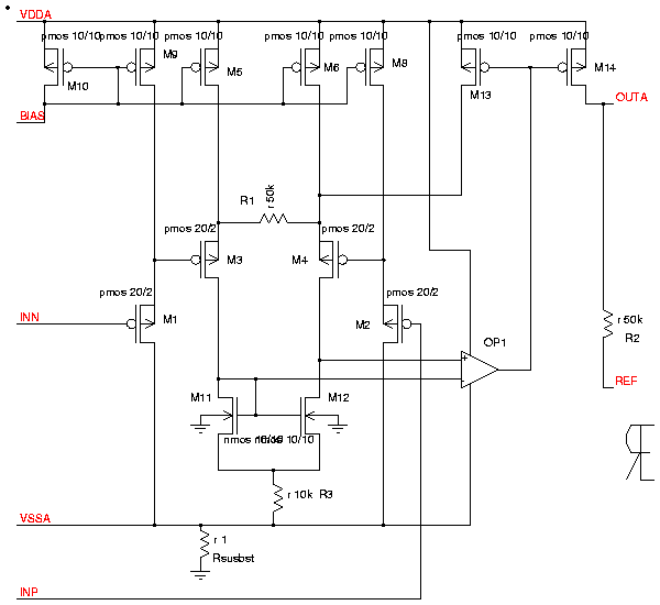
Fig. 4: Assymetric instrumentation amplifier
Now the feedback signal is no more the difference of two current but the replica of the current flowing in R2 itself (4). Since this circuit only can source but not sink current the transfer function becomes assymetric now.
M13 and M14 matching errors change the gain of the amplifier but not the offset at VIN=V(INP)-V(INN)=0V. However operating M13 and M14 close to subthreshold will still bulge the tolerance range close to 0V.
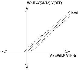
Fig. 5: Transfer function of the assymetric instrumentation amplifier
solid: ideal characteristic.
dashed: tolerance field including the matching of the inpu stage.
dotted: tolerance field additionally considering poor matching of M13 and M14 at low currents.
The price for this kind of error reduction is poorer supply rejection and common mode rejection at high frequencies due to the introduction of assymetries!
As an alternative of this kind of dirty method CMOS technology offers the possibility of chopping the amplifier to reduce offsets and still maintain a symmetrical circuit.
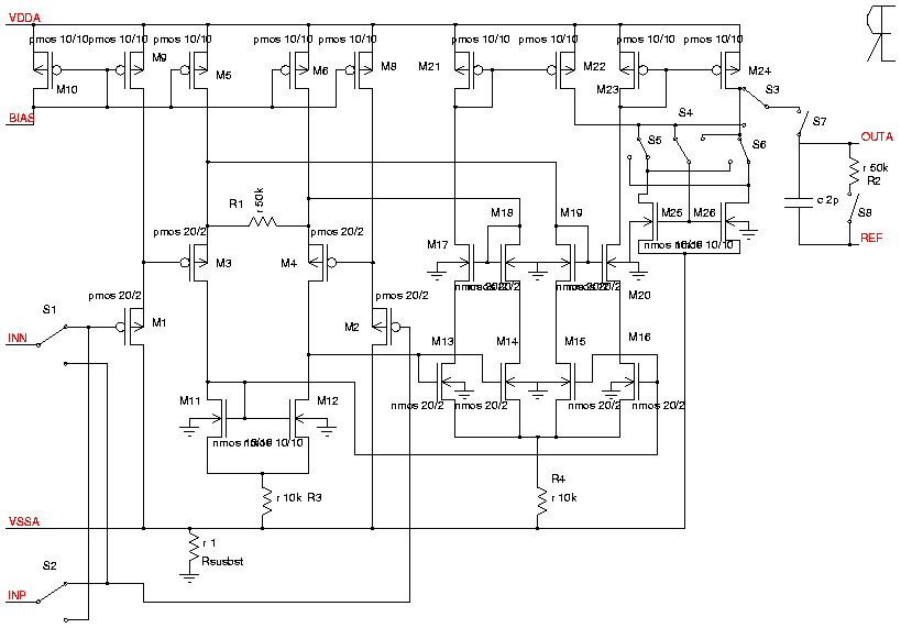
Fig. 6: Chopper stabilized instrumentation amplifier
S1 to S4 switch simultaneously. Since the symmetry is broken at M25 and M26 the current mirror must be chopperstabilized additionally. Usually this is done by switches S5 and S6 at double the clock frequency of switches S1 to S4.
S8 and S8 can b used to reduce the clock noise at the output disconnecting the output while the amplifier settles again after changing the switches S1 to S6. A typical clock scheme looks as follows:
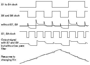
Fig. 7: clock scheme, theoretical clock feed through and feed through minimization with S7 and S8
The output only works accurately as long as the transistors M24 and M26 operate in saturation. Therefore the output can not work rail to rail. If rail to rail operation is desired a 2 stage concept is needed (4).
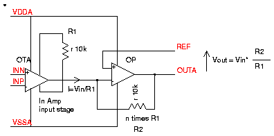
Fig. 8: Instamp with inverting buffer to achieve rail to rail output capablity
The additional beauty of this 2 stage design is that the output of the first stage always operates at the same output voltage and early effects degrading the performance are avoided. Besides that there is no more current flow into the reference pin REF.
Literature
1. Tietze, Schenk. Halbleiterschaltungstechnik. Springer 1980
2. Linear Integrated Circuits data book, Motorola Inc. 1971
3. National Semiconductor Linear Data Book, 1982
4. W. G. Jung, Op Amp Applications, Analog Devices 2002