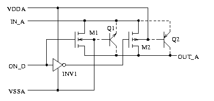
Fig. 1: The most simple CMOS voltage switch
Fig.
1: The most simple CMOS voltage switch
The
circuit shown in figure 1 works acceptably well as long as the analog voltages
do not exceed the range VSSA-Vbe to VDDA+Vbe.
Below
VSSA-Vbe parasitc bipolar transistor Q1 gets activated bypassing the switch
even if M1 and M2 are off.
Above
VDDA+Vbe Q2 bypasses M2.
So
this circuit can only be recommended for internal signals the circuit designer
has perfectly under control.
For
signals comming from outside the chip or from other supply domains the
following circuit is recommended.
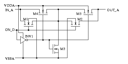
Fig.
2: Improved CMOS switch
The circuit of figure 2 is a T-topology. Even if M1 and M4 are bypassed in off state by parasitic transistors M3 will short circuit the undesired signal to ground. Even if the open switch signal rejection from IN_A to the drain of M3 is not perfect it usually is good enough to prevent activation of the bulk parasitics of M2 and M5.
Trying to build similarly simple topologies in bipolar technologies almost certainly fails. To illustrate the reasons let us see figure 3.
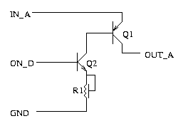
Fig.
3: Analog switch using bipolat transistors
To
connect IN_A with OUT_A the voltage drop from emitter of Q1 to collector
of Q1 must approach 0V. In this saturated operating mode part of the base
current will flow from the base into the collector. As a consequence the
voltage at OUT_A will always deviate from the input voltage at IN_A. The
deviation depends on:
- ratio of dopings in the emitter and the collector of Q1
- ratio of collector-base junctioon area and emitter-base area
- temperature
- base current
Typical
deviations are arround 100mV.
Besides
this offset the base current of Q1 flows into the emitter and the collector
of Q1. Depending on source impedances (driving IN_A) and load impedances
(driven by OUT_A) the base current superimposes the signal to be switched.
A more accurat way of switching voltages in bipolar technologies is using amplifiers driving the same output stage. A multiplexer can be built by just biasing one of the differential stages while the other one is high resistive.
Fig.
4: Analog volltage multiplexer using bipolar transistors.
The
circuit works well as long as the logic HIGH levels (driving the base of
Q7 or Q8) are lower than the analog voltages (IN0_A, IN1_A) to be switched.
Drawbacks of this solution are:
- Minimum analog voltage must be higher than logic HIGH level.
- Q1, Q2, (Q3, Q4) Q5, Q6, Q12 create a unity gain amplifier.
- Amplifiers get slow because they must be compensated for unity gain.
- Offset in the range of +-1mV.
With
slight modifications the circuit can be used for AM and DSB (dual side
band, no carrier) modulators.