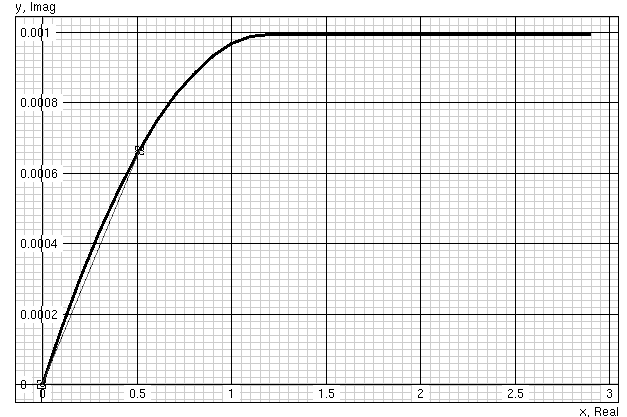
Fig. 1: Output characteristic of an nmos transistor with Vgs=1.5V
MOS transistors have a saturated operating range and a non saturated operating range. In the non saturated (sometimes called triode operating range) the MOS transistors have a characteristic similar to a resistor. On the following plot this is the range between Vds=0V and Vds=0.5V.
Fig. 1: Output characteristic
of an nmos transistor with Vgs=1.5V
Simply applying a fixed gate voltage accuracy suffers from the fact that the MOS transistors have a significant production spread and temperature coefficient. The Rdson may well change +-40% by production spread and +-30% due to temperature changes from -40°C to 150°C. To overcome this problem the gate voltage can be regulates such that a reference cell is operated at a defined Vds and a defined Id. This way the Rdson of the reference cell becomes Ron=Vds/Id
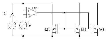
Fig. 2: Tunable precision
resistor in regulation loop
Now the Rdson of M2 is:
R2 = V/I *Wm2*Lm1/(Lm2*Wm1)
accordingly Rdson of M3 of course calculates as:
R3 = V/I *Wm3*Lm1/(Lm3*Wm1)
Usage of the circuit:
There are many possible usages ranging from tunable attenuators to AM modulators or even analog filters. As an example let us see a simple attenuator:
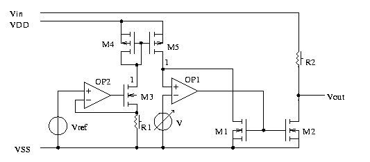
Fig. 3: Simple tunable MOS attenuator
The reference current calculates as:
I=Vref/R1
Assuming M4 and M5 are designed with equal width and length Rdson of M1 becomes:
Rdson = V*R1/Vref
For simplicity assuming M2 has the same size as M1 the attenuation becomes:
Vout=Vin*Rdson/(Rdson+R2)
Vout=Vin*(V*R1/Vref) / (V*R1/Vref + R2)
All transistor parameters
of M1 to M5 (almost) cancel. Attenuation depends on the ratio of R1 and
R2 and the tuning voltages V and Vref. Since resistor matchings are well
reproducable on integrated circuits this leads to an integratable circuit
using standard CMOS technologies.
Making R2 high resistive
compared to the Rdson of M2 this circuit becomes a nice AM modulator with
the carrier supplied at Vin and the modulation supplied as input voltage
V.
The circuit can also be enhanced
to become a dual side band (rejected carrier) modulator or in other words
a 4 quadrant multiplier.
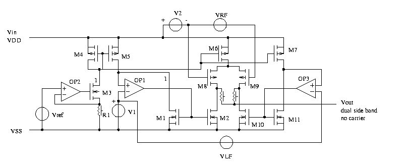
Fig. 4: 4 quadrant CMOS
analog multiplier
Now M8 and M9 provide an
inverted current signal converted into inverse voltages again by M2 and
M10. The input signal (carrier) is applied differentially by VRF between
the gates of M8 and M9. V2 just is needed to establish the operating point
of the differential stage M8, M9.
The lof frequency signal
also is applied as a differetial signal between the input of OP1 and OP3.
V1 just defines the DC operating points of M1, M2, M10, M11.
Since this circuit now matches
a gm with an impedance defined by V1, Vref and R1 the circuit has a certain
spread of the gain. This can be improved by degrading gm of M8 and M9 by
resistors of the same kind as R1.
Eventually the signal is
reassembled by two matched resistors connecting the output to the drains
of M8 and M9.