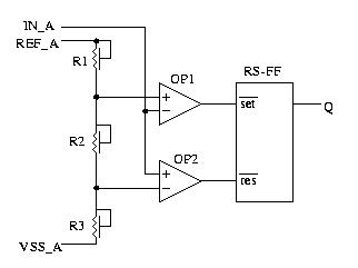
Fig. 1: Precision trigger circuit with two amplifiers and RS flip flop.
Fig. 1: Precision trigger
circuit with two amplifiers and RS flip flop.
This circuit can be implemented in MOS as well as in bipolar technologies.
MOS technology allows the
following low power variant of the circuit shown in figure 1:
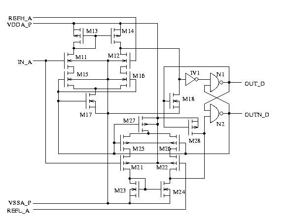
Fig. 2: MOS comparator with bias-self-turn-off
To understand how it works
let us assume a rising edge at input IN_A.
The reference voltage REFH_A
is higher than REFL_A. As long as the input voltage is below REFL_A the
output OUT_D is low and OUTN_D is high. Long channel M17 is on. Short channel
M15 and M16 are on too. The opposit comparator M21 to M27 is unbiased.
Long channel M28 is on to prevent the input of N2 from floating.
As long as the input signal
IN_A is below the threshold of M11 no bias current flows through the path
M11, M13, M15, M17. M12 and M17 pull the input of IV1 low and the flip
flop N1, N2 remains as before.
Once IN_A exceeds the upper
reference REFH_A M11, M13, M14 turn on. The flip flop N1, N2 switches.
OUT_D becomes logic 1 and OUTN_D becomes logic 0.
After switching the flip
flop M15, M16, M17 turn off thus eliminating the current flow in the first
comparator again. Long channel M18 turns on to prevent the input of IV1
from floating.
Now the second comparator
is active. Long channel M27 and short channel M25 and M26 bias the differential
stage M21, M22. Since the signal at IN_A is significantly higher than REFL_A
the current flow through M21, M23, M24 is very low or almost 0.
A falling edge at IN_A will
turn on M21, M23, M24 when IN_A drops below REFL_A. This will flip the
flip flop N1, N2 and then turn off the bias through M27 again. Now we are
back to the state we started from.
The corresponding current
consumption can be seen below.
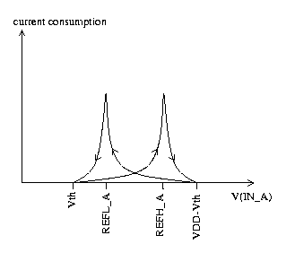
Fig. 3: Current consumption
w.r.t. input voltage at IN_A
WARNING: The circuit of figure 2 was patented by ST-Microelectronics 1994 (EP 0 640 259 B1). Please check license agreements before using it.
Since building comparators or amlifiers with low offset is expensive a cheaper solution is tempting.
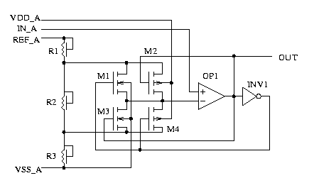
Fig. 4: Precision trigger
with one comparator and a reference switch
Here the output of the amplifier
switches the transmission gates M1 to M4 to create the hysteresis. The
circuit has the risk of oscillation if the capacities of the switches are
not balanced and the slopes of the amplifier output capacitively (via the
gate capacities of M1 to M4) feed back to the inputs of the amplifier.
To solve the problem the
amplifier OP1 can be made gain-1-stable (see stability considderations
of amplifiers with feed back). This is the most secure solution that
provides stability no matter which parasitic capacities are encountered
in the switches. Frequency compensation however reduces the speed of the
circuit.
Alternatively the capacities
of M1 to M4 can be minimized so far that the cut of frequency of the unintentional
feed back gets too high to fall into the gain-bandwidth product of OP1.
Usually a combination of
both methods is used.
The circuit can only be implemented in MOS technologies. Bipolar technologies suffer from base currents and saturation voltages. Therefore the switches can barely be implemented in a bipolar technology.
Since resistors are large it may be desireable to eliminate R2 and R3. The following circuit works fine in case a reference current created by Vref/R is available.
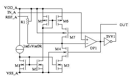
Fig. 5: Deriving the second
reference by a current generator and a resistor.
Since M7 and M4 switch currents in stead of voltages this concept can be used for MOS as well as bipolar implementations.
The following figure shows
a fully symmetrical implementation as often used for differential line
receivers.. Due to the symmetry of the design most parasitic capacities
cancel (provided the layout is symmetrical accordingly). Since most
differential receivers are intended to switch with a certain offset M5
and M11 have been added to create an offset.
To avoid rectification at
the well diodes of the resistors R1 to R4 preferably should be implemented
as poly silicon resistors.
VREF_A intends to define
the DC operating point of OP1.
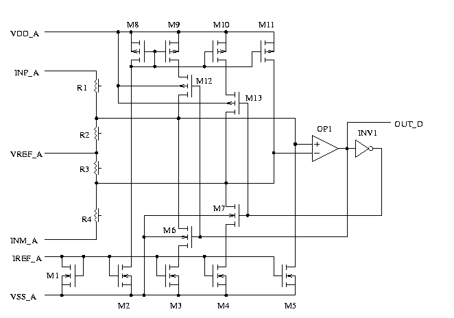
Fig 6: Concept of a high
speed CAN receiver.
This circuit can be built in bipolar technology as well.