Most Common Test Pulses

(Published Sept. 2006, Update May 12 2017)

MIL-STD883E HMB, AEC-Q100-002

The most frequenty used pulse is the human body ESD pulse according to MIL-STD-883E. It uses the following test setup:

MIL883E_HMB.gif
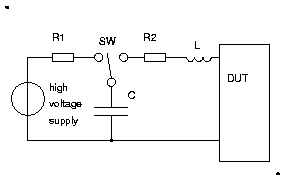
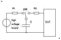
Fig. 1: MIL-STD883E HMB model
C=100pF, R2=1500 Ohm


In MIL-STD883E the power supply charges C1 via R1 to several kV. The energy is stored in a capacitor C with 100pF. When the switch is thrown to the right side the energy stored in C discharges into the device under test (DUT) through R2.
Since the ESD protection clamps the voltage to some 10V the peak current flowing through R2 can be estimated as:

Ipeak = V0 / R2
Ipeak = V0/ 1500 Ohm

(Example: V0=8kV -> Ipeak=5.33A)

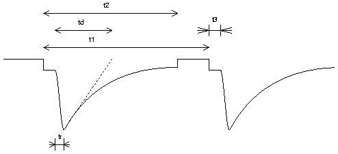
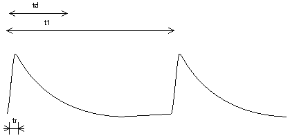
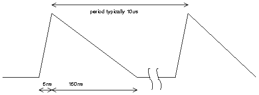
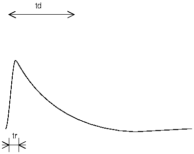
The voltage at C and thus the current though R2 decays approximatelly exponentially with a time constant of:

T = RC

I(t) = V0/R2 * exp(-t/T)
I(t) = V0/R2 * exp(-t/150ns)

(This is not the full truth because there are some parasitic inductances involved that add some ringing to the signal. MIL-STD883E allows up to 10ns rise time at the DUT. But for a rough estimation of the energy delivered to the DUT the description of I(t) as a exponentially decaying current is not too bad.)

During the ESD test the DUT is unsupplied. ESD tests give no indication of latch up robustness!

IEC1000

IEC1000 originally was intended for board tests. IEC1000 uses a similar setup as MIL-STD883E but chooses different values for C and R2. Besides different component values IEC1000 limits the parasitic inductance in series with the resistor R2 to such low values hat the rise time of the current is arround 0.7ns to 1ns. This aggressive rising edge together with the response time of the protection means that IEC1000 is significantly harder to meet than MIL-STD883E. The changed parameters lead to:

Ipeak = V0 / R2
Ipeak = V0 / 330 Ohm

(Example 8kV -> Ipeak = 24A)

T = R2*C = 150pF * 330Ohm = 50ns

I(t) = V0 /330 Ohm * exp(-t/50ns)

Maschine Model, AEC-Q100-003, Charged device model (CDM)

There are several different maschine models used for ESD testing. Basic idea is to model the ESD pulse created by the mechanics of a conducting handler. The arm of the handler is assumed to maily be an inductance L. The damping resistor R2 varies depending on the model used between some Ohm and some 10 Ohm. The inductance L varies between 1uH and 2.5uH.

CDM (charged device model) tries to simulate the air discharge rght into the pin of an IC. The circuit is similar to MM but the parameters differ dramatically.
MM-model.gif
Fig. 2: Mashine Model setup

Model
C in pF
R2 in Ohm
L in uH
AEC-Q100-003
200
less than 1
about 1
Philips
200
25
2.5
CDM, AEC-Q100-011
4pF to 30pF
1
as low as possible,  L<50nH

The signal I(t) becomes:

I(t) = V0/(L*wd) * exp(R*t/2L) * sin(
wd*t)

with

wd = SQRT(w2-a2)

Due to the excitation of an LC tank circuit MM and CDM suffer from poor reproducability!

About CDM:
The wide range of C in the CDM (4pF to 30pF) is a matter of the IC package used. 4pF correspond a very small package (such as SO8). 30pF corrspond a large package like 80 pin TQFP. The test is carried out placing the IC on a grounded metal plate and directly zapping into the pin. The capacity C is the spread capacity between the chip inside the package and the grounded metal plate. Since this is a fairly vague description the standard requires a complex calibration procedure to meet a certain pulse shape rather than using a setup with discrete components.

ISO7637, DIN40839

These standards describe a potpoury of pulses used for automotive applications.
Pulse 1, 2a and 6 model the flyback pulses of inductive loads. Typically these pulses are found on automotive supplies. The pulse source has a certain impedance (ranging from 1 Ohm to 50 Ohm). So the DUT or external components belonging to the application can clamp or attenuate the pulses.
Power drivers of loads connected to an automotive supply or bus interfaces like LIN subbus will see these pulses as well through the impedance of the load.
High side switchs supplied directly from the battery will be directly impacted by these pulses. Usually they will protect themselves by dumping the energy into he load rather than by absorbing the energy in the silicon.
pulse1.gif
Fig. 3: Pulse 1

pulse2.gif
Fig. 4: Pulse 2a, Pulse 6

Pulse 3a, 3b represent capacitive coupling of a high voltage ignition line into the pin under test. The source impedance is 50 Ohm. The pulses are applied to the system using a capacitve coupler wit about 300pF. Usually these pulses come in bursts of up to 10000 pulses with 100kHz. Pulse 3a is negative. Pulse 3b is positive.
The energy content of one pulse with 100V roughly corresponds an MIL-STD883 HMB pulse of 2kV.
pulse3b.gif

Fig. 3: Pulse 3b

Pulse 5 and 7 model the so called load dump. These pulses occurre when the alternator is running at high load current (e.g. charging the car battery) and then the battery gets disconnected. Usually a single pulse is tested.

pulse5.gif

These tests are carried out while the IC is supplied. Therefore these pulses can create a latch up.

The following table summarizes the automotive pulses:

pulse
source
rise
 tr
duration
td
period
t1
t2
t3
typ test ampl.
1
10 Ohm,
30 Ohm,
50 Ohm
typ. 1us
50us to 2ms
>0.5s
200ms
<100us
down to -300V
2a
2 Ohm,
4 Ohm,
10 Ohm,
30 Ohm,
50 Ohm
typ. 1us
50us to 500us
>0.1s


up to 300V
3a
50 Ohm, 300pF
5 ns
150ns
>10us


-50V to -400V
3b
50 Ohm, 300pF
5 ns
150ns
>10us


50V to 400V
5
0.5 Ohm to 10 Ohm
10 ms
40 ms to 400 ms
single


up to +200V
6
30 Ohm
60 us
300 ms
single


7
0.5 Ohm to 10 Ohm
10 ms
50 ms to 400 ms
single


down to -200V

The table leaves a lot of uncertainties. Which impedance, which pulse amplitude and which external circuitry really is to be used must be agreed with the customer. Besides that it must be clarifierd whether the device under test has to function during the test or may only not be destroyed while malfunction is accepted.
The energy of most of these automotive pulses is so high that plain ICs without external circuitry will be destroyed by the heat generated. Only pulse 3a, 3b can be survived for a certain time by optimized ICs without external components.