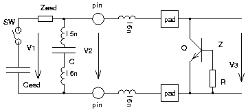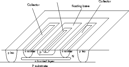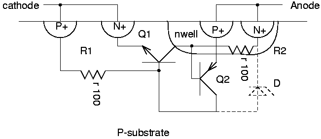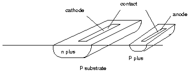
Fig. 1: Substrate zener diode
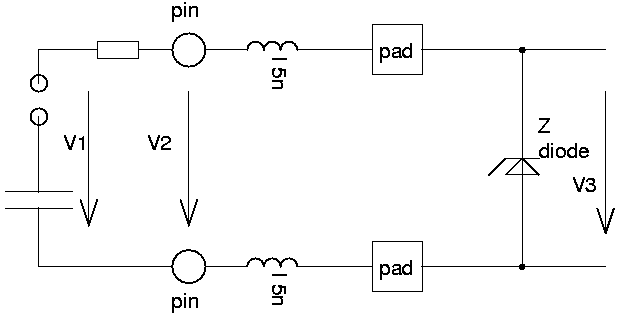
Fig. 2: ESD protection with zener diode.
The substrate zener diode will acceptably well protect NMOS transistors with low doped drain extension. If it is used to protect low voltage NMOS transistors the spacing between the n-plus (cathode) and the p-plus (substrate contact) must be reduced such that the depletion area reches the p-plus region before the NMOS transistors break. In extreme cases n-plus and p-plus can touch to obtain a break down voltage of only a few volt.
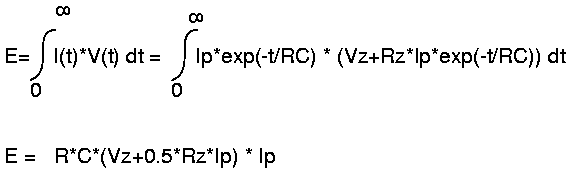
The following plot shows the voltages V2 and V3 of such a protection.
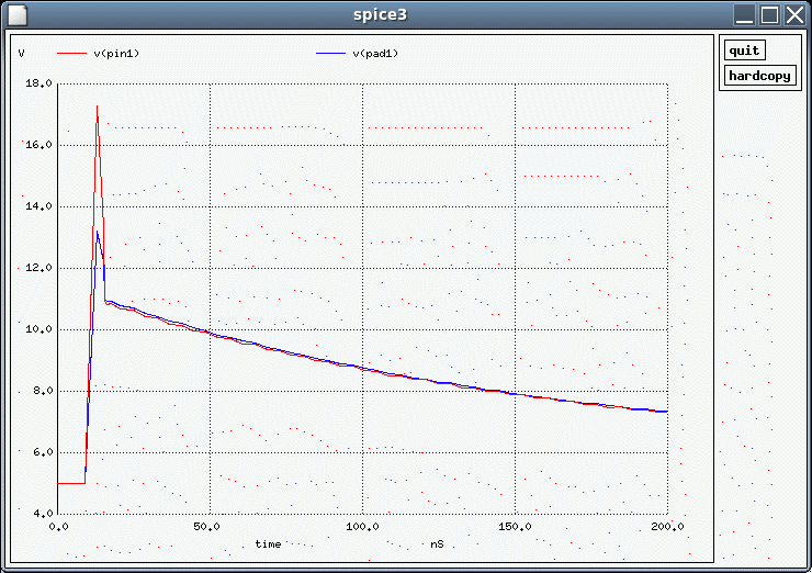
Fig. 3: Simulation of a zener protection