Limiting stage before
the secundary ESD protection
(Published Oct. 2006, Update May 12 2017)
Even the most
rigid ESD protections have a certain response time. The following
figure shows the response of a thyristor protection to a 4kV MIL883
human pody pulse.
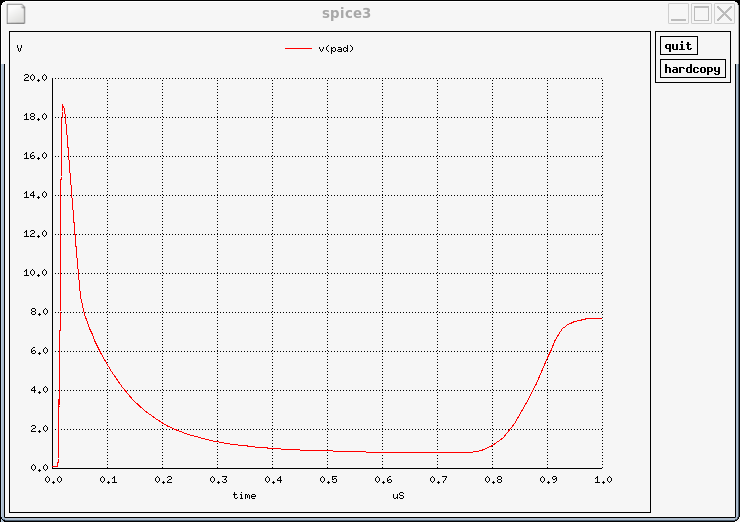
Fig. 1: Voltage at the pad of a thyristor protection
It is clearly visible that the hold volteg below 2V and the release
voltage of 8V is suitable for a 5V CMOS technology. The response delay
creating a peak voltage of 18V however would be fatal for the gates of
these CMOS gates. Therefore the energy must be further reduced adding a
secundary ESD protection.
The most simple way would be to add a low pass filter taking away the
peak.
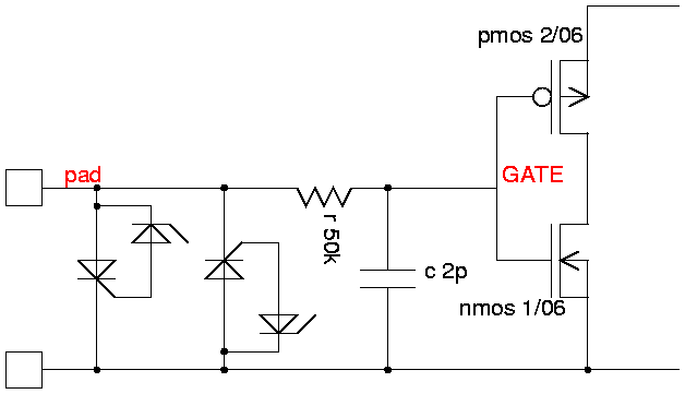
Fig. 2: CMOS gate protection
This very basic vircuit works fine as protection but it adds a
significant low pass to the input. Besides that resistors of 50K and
capacitrs of 2pF are not really a cheap solution on an IC. Therefore
the example given is a plain educational example.
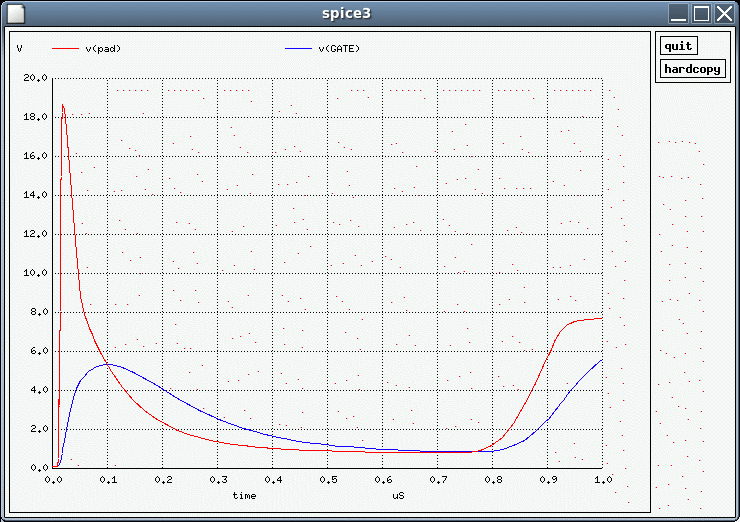
Fig. 3: Performance of the demonstration circuit adding a low pass
before the gate.
On ICs active devices are prefered in stead of using area consuming
capacitors. For the current limiting element the fundamental
requirement is that it can survive a pulse of about 20V while the other
side of the 'currnt limiter' is held at 5V or less by an appropriate
secundary ESD protection.
Polysilicon
resistors
In most cases
this is the prefered choice if polysilocon resistors are available in
the technology. Typical values range from some hundred Ohm to several
kilo-Ohm.
Resistors always require a secondary clamp at the gate to be protected.
Polysilicon resistors are embeded in SIO2. So the specific
thermal impedance (rth*area) is fairly high and the resistor
has to be designed sufficiently large (e.g. if it is chosen very low
resistive).
Diffused
resistors
In technologies
not providing polysilicon resistors diffused resistors are often used.
Here the parasitic diodes have to be taken into account. Usually these
diodes are either connected to p-substrate (n-resistors in substrate)
or to VDD (p-resistors in an nwell). The parasitc diodes should be high
resistive enough to keep the ESD energy in the primary protection but
lower resistive than the resistor itself to act as a clamp on the
GATE-side of the resistor.
Diffused resistors have a much better thermal impedace than polysilicon
resistors. This may be a significant advantage for resistor values
below 300 Ohm used at outputs or bidirectional ports.
High voltage
MOS
If NMOS
transitors with a drain extension exist in the technology the following
structure can be used:
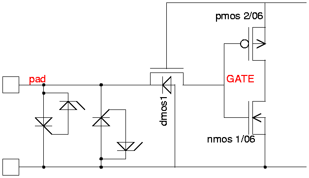
Fig. 4: DMOS limiter
The voltage at the source can not exceed the supply voltage VDD-Vth of
the transistor dmos1. The diode is the drain-bulk diode of the
protection transistor. usually it is intentionally designed with a high
path resistance to keep the ESD energy of negative pulses in the anti
parallel thyristor. To clamp negative pulses at the source of DMOS1 the
diode must nevertheless be less resistive than Ron of DMOS1 (There is a
second bulk diode to the source that is not shown in the symbol but
should not be forgotten).
For propper operation the threshold of dmos1 must be less than the
threshold (-Vth) of the pmos transistor. In practical circuits the gate
of dmos1 often is driven by a higher voltage than the source of the
pmos transistor.
Special care must be taken about drain-source leakage, As long as he
bulk is tied to ground this is not a problem. In case the bulk is
connected to the source the leakage and the drain-bulk capacity may
require further protections at the gate of the CMOS transistors to
prevent high gate voltags due to DMOS1 leakage or capacitive feed
through.
Of course the circuit can be inverted using a high voltage PMOS and
connecting the gate to ground in stead of a high voltage NMOS.
Somtimes combinations with an NMOS limiting positive pulses and an PMOS
limiting negative pulses are found.
EMC: Please consider this
circuit is very nonlinear and will rectify RF!
Cascodes
Some technologis
offer fully isolated transistors (the bulk can be connected where ever
the designer wants). This gives the oportunity to stack drain-bulk
diodes to increase the break down voltage (provided VDD follows the ESD
pulse up to a certain point where it is clamped).
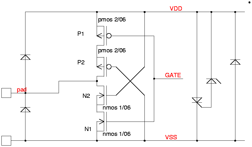
Fig. 5: Stacked transistors
In the output stage shown the series of NMOS transistors will break
either reaching:
V(pad) > 2*| VBRdrain-bulk-N |
or
V(pad) > VDD+ |VDGmax-N |
The same applies to the PMOS transistors. The conditions for
destruction are either
V(pad) < VDD-2*| VBRdrain-bulk-P|
or
V(pad) < -|VDGmax-P|
The bulk diodes can intentionally be made high resistive enough to
dissipate most of the energy in the protection structure rather than
inside the bulk diodes.
This topology becomes especially attractive if signal pad is clamped to
VDD and VSS by diodes. This makes VDD follow the pulse until the VDD
rail clamp begins to hold VDD down.
Combining high voltage transistors (N2, P2) with low voltage
transistors (N1, P2) is also very attractive. Since high voltage
transistors are much larger they have high parasitic capacities. Adding
zener clamps parallel to N1 and P1 is suggested in this case to limit
capacitive feed through that otherwise still could harm N1 and P1.