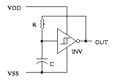
Fig. 1: Most simple RC oscillator
Relaxation oscillators create
non sinusoidal signals. Usually the output signal is rectangular or some
kind of triangular. As an amplifier most of these designs use trigger stages
that flip between two operating points. The circuits usually are robust
and cheap.
Fig. 1: Most simple RC oscillator
To eliminate the tolerances of the schmitt trigger the following circuit can be used.
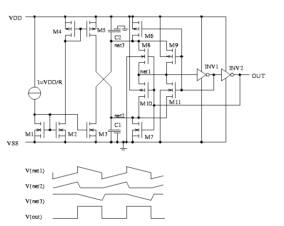
Fig. 2: Oscillator without
schmitt trigger accuracy impact.
Usually both capacitors are
designed equal and both charging current are equal. This way the capacitors
are alwas charged from 0V to the threshold of inverter INV1 or from VDD
to the threshold of inverter INV1. Changes of the MOS transistor parameters
impact the duty cycle, but not the frequency.
The circuit requires a bias
current proportional to VDD to become supply voltage independent.
If a stable duty cycle is needed additionally a precision schmitt trigger must be used.
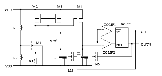
Fig. 3: Oscillator with
stable duty cycle
The source voltage of M1 is the reference the capacitors alternately are charged to. Since the charge current is proportional to the reference voltage the reference voltage itself cancels in the equations of the frequency (assuming unlimited fast comparators).
Bipolar designers will mind the high number of transistors. The size of a minimum bipolar transistor often is as big as a complete flip flop in MOS technologies. Therefore bipolar designers sometimes use small, but less robust circuits.
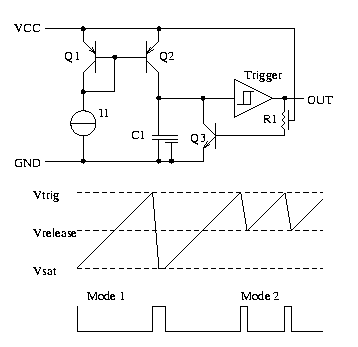
Fig. 4: Low cost bipolar
oscillator
The design uses a simple
bipolar
schmitt trigger designed with a stable upper threshold. Depending on
the turn off delay of Q3 the oscillator may run in two different modes.
If the turn off delay is
longer than the time needed to discharge C1 from the lower threshold of
the trigger stage to 0V (or almost 0V) the oscillator runs in mode 1. If
the turn off delay of Q3 is shorter the oscillator operates in mode 2 or
something between the two modes. The risk of the design is that the turn
off delay depends on various parameters:
- Minority
carrier life time of the process
- Chip
temperature (changes B and minority carrier life time)
- gain
B of Q3
- Peak
discharge current (Q3 may go into inner saturation)
- Sinker
resistance
- Base
drive current of Q3
Concluding we can see the
circuit is cheap but hazardous.
The following figure shows a nice RC oscillator with one capacitor.
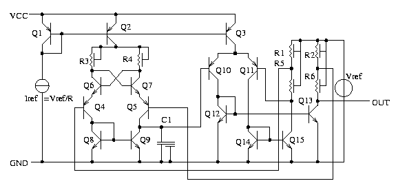
Fig. 5: Symmetrical bipolar
RC oscillator
The circuit charges and discharges
C1 through Q5 or Q9. Comparator Q10, Q11 switches between charging and
discharging. The swing is defined by the current through R1 and R5. R1
and R2 must be sized such that Q5 does not saturate. Usually the amplitude
at R2 is in the range of 100mV to 300mV.
Without Q6 and Q7 the oscillator
would have an undesired stabel point: Assume Q10 and Q11 carry the same
current. In this case Q4 and Q5 (without the flip flop Q6 and Q7) would
exactly be balanced and the capacitor would neither be charged nor be discharged.
In this point the circuit without Q6 and Q7 would become a two stage OTA
with a dominant pole created by C1 in the feed back path. Q6 and Q7 are
needed to prevent this operating point. R3 and R4 should be scaled to obtain
a drop of 100mV to 300mV so that Q6 and Q7 will not saturate.