Level shifts for logic signals
Upadate May 13 2017
Reasons for using level shift circuits
In most modern
digital systems sever supply voltages are existing. Usually the core
voltage is fairly low (for instance 1.1V) while the external circuits
and the ports operate at higher voltages (for instance 3.3V or 5V).
The transistors
in the core operating at low voltage are very small and fast while the
transistors at the ports are bigger and more robust.
In some cases signals have to be carried into completely different
supply domains. This could require shifts from for instance 0-5V into a
second domain of 12-17V.
Depending on reliability constraints level shifts can be built
dynamically (AC coupled) or static (DC coupled). Dynamic shifters (AC
coupled) often have the problem of an undefined initial state. Usually
AC coupled shifters synchronize after some pulses.
High reliability requires DC coupled shifters that avoid the problem of
starting out of an undefined state.
The following circuits are examples but surely do not cover all
possible implementations.
Simple DC
level shift between two supplies with same reference ground
The following
example is a typical shifter between two logic supplies that refer to
the same ground or two grounds with potential differences in the range
of not more than some hundred mV.
To work correctly the NMOS transistors M1 and M2 must ander any
circumstances be stronger than the PMOS transistors M5 and M6.
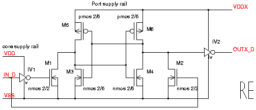
Figure 1: most simple level shift
M1 and M2 may have a thin gate oxide as a core transistor but require
drain extensions like port transistors. M3 to M6 and inverter IV2 are
high voltage port transistors (drain extension and thick gate oxide).
Level shift
for completely different supplies
In high voltage
ICs and chargepumps the supplies as well as the 'grounds' may differ.
The following static shifter is quite reliable but usually slower than
a capacitive shifter.
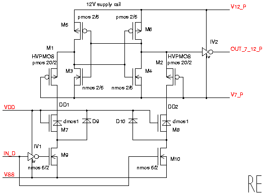
Figure 2: levle shift between completely different supplies
In the circuit shown in figure 2 M1, M2, M7, M8 are high voltage
transistors in the sense that they must be able to sustain a high drain
source voltage of V12_P-VSS.
The gates of M1 and M2 are stressed with V12_P-V7_P, which usually is
much less.
The gates of M7 and M8 are stressed with VDD-VSS.
M9 and M10 are low voltage transistors. To protect them against leakage
currents of M7 and M8 it is recommended to use diodes D9 and D10. D9
and D10 can simply be implemented using antenna diodes sitting in the
nwell of inverter IV1.
Switching
behaviour:
Let us assume M5
is on and M4 is on. So OUT_7_12_P is high (12V). To change the state we
turn on M9 and turn off M10. The current will flow through M5, M1, M7
and M9. The drain of M5 moves to V7_P+Vth of M1. If M1 is sufficiently
wide the latch will flip turning off M5 and turning on M3. Now the
voltage at the source of M1 approaches V7_P and M1 turns off again.
With M1 turned off the current through M7 and M9 returns to 0A.
Simultaneously M6 turns on and M2 turns on. The current through M6 must
pull up net DD2 from about 0V to V12_P (12V in our example). Since M2
and M8 are large high voltage transistors the stray capacity of net DD2
and the voltage swing of this net limits the switching speed.
Variations
of the Circuit
The same circuit
can be used to carry signals from the high domain to the low domain. We
simply have to change the polarity of the transistors and put the latch
on the low voltage side.
To make it even more interesting let us build a high voltage power
output with a swing that is limited by Vds but not by Vgs.
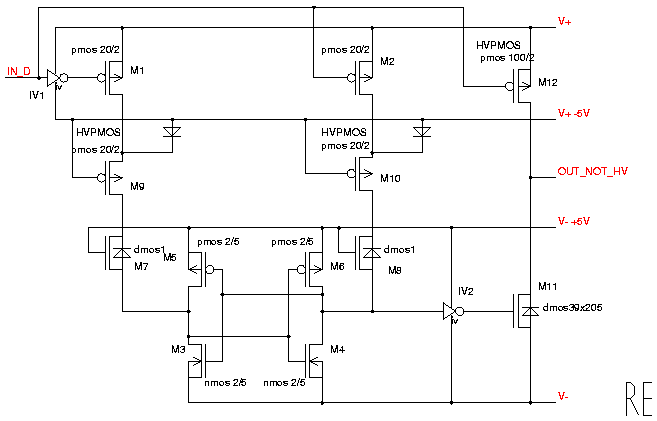
Fig. 3: High voltage port driven from the high supply domain
Figure 3 uses the same levelshift as shown in figure 2 except that now
the domain acting as input and the domain we are shifting to is
exchanged. The voltage swing at OUT_NOT_HV only is limited by the Vds
capability of M11 and M12. The maximum gate voltage of M11 and M12 is
not crtical because there the voltage swing only depends on the
supplies V-+5V and V+-5V.
Clock Shifter
For fast clock
signals the static shifters of figure 2 and figure 3 are not a good
choice because the bulky high voltage transistors with high drain to
substrate capacities and the wide signal swing at their drains create a
lot of delay. Therefore for fast but repetitive signals capacitive
shifters are the better choice.
Typically such shifters are used for chargepumps and similar
applications. In a chargepump loosing the first one or two pulses
usually is not a problem and dynamic circuits are acceptable.
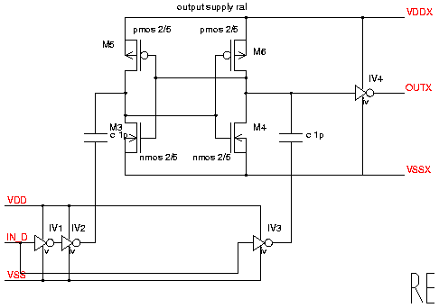
Fig. 4: Capacitive level shift
To operate savely the swing provided by IV1 to IV3 must be sufficient
to take the latch from VDDX to below the metastable point of the latch
and from VSSX to above the metastable point of the latch. If the latch
is designed perfectly the metastable point should be at (VDDX+VSSX)/2
and the swing needed would be (VDDX-VSSX)/2.
Since there is production spread (M3 and M5 never match because they
are of different type!) it is reasonable to design (VDDX-VSSX) <
1.3*(VDD-VSS).
Consider there is some charge loss due to current taken from the
capacitor until the latch flips and due to stray capacities on the
upper side of the capacitor.
Looking at the layout of the critical wires is always worth while. Your
analytic brain and your own eyes are better than trusting any DRC or
LVS.
The Initial
Condition Problem
Once they synced
in capacitive level shifts work most reliable when they are symmetrical.
Some people try to solve the initial condition problem by making the
latch assymetrical. I personally would not take this chance anymore. I
have already seen power supplies blow up due to double pulses caused by
capacitive level shifts. Fire works in power supplies are a really
impressive experience what one ppm failure rate means! Rather build a
slow DC-coupled shifter for the correct initial state and combine it
with a capacitive shifter acting as speed up if you must solve the
initial state problem.
Last Words
Have fun
building your own circuits. Always remember going from one supply
domain to the other stick with differential signals as best engineering
practice. Single ended circuits will fail as soon as the supplies
bounce!
Keep ESD in mind. Your level shifters are more exposed to ESD than
anything else in the chip!