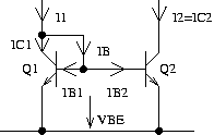
Fig. 1: Simple NPN Mirror
R=Vearly / I
with Vearly being
the early voltage of the transistors used and I the current flowing through
the mirror.
Example: Typical
40V NPN transistors usually have early voltages as high as 50V. Operating
at 10uA this leads to a resistance of 5M Ohm.
Fig. 1: Simple NPN Mirror
The base voltage of Q1 can be aproximated by:
Vbe = VT*ln(IC1/I0) with I0 being the diffusion current. I0 is strongly temperature dependent.
Since Q2 operates at the same base voltege as Q1 the collector current of Q2 becomes:
IC2 = I0*exp(VBE/VT)
IC2 = I0 * exp(VT*ln(IC1/I0) / VT)
IC2 = I0 * exp((ln(IC1/I0)
IC2 = IC1
This of course only applies if Q1 and Q2 have the same emitter geometry and the same temperature.
The input current I1 of the mirror consists of IC1, IB1 and IB2. IB1 and IB2 are the base currents of Q1 and Q2. Since IC1=b*IB1 and IC2=B*IB2 Tthe current calculate:
I1/I2 = (IC1 + IB1 + IB2) / IC2
I1/I2 = (B*IB1 + IB1 +IB2) / B*IB2
since both transistors are assumed to be equal IB1 and IB2 are equal too.
IB1 = IB2 = IB
Using this experession the equations simplify:
I1/I2 = (B+2) / B
I2/I1 = B/(B+2)
So due to the limited gain of the bipolar transistors the mirror is less than perfect. The current ration is not equal 1.
To reduce this error a modified version of this mirror can be used:
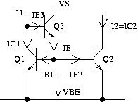
Fig. 2: Boosted NPN Mirror
In the circuit shown above Q3 is used to reduce the error caused by the base currents of Q1 and Q2. Now I1 consist of the base current of Q3 and the collector current of Q1. This leads to:
I2/I1 = B / (B+2/B)
I2/I1 = B2 / (B2 +2)
Assuming a gain of 100 the error caused
by the base current reduces from 2% in figure 1 to 0.02% in figure 2. Unfortunatelly
there is no free lunch!
We have to pay this improvement by a stability
problem! Q1 and Q3 create a regulation loop. In this loop Q1 acts as an
inverting voltage gain stage while Q3 is a non inverting unity gain amplifier.
The poles of the loops can roughly be calculated.
At the collector of Q1 (the output of
the foltage gain stage) we will find an impedance of about:
Rq1 = Vearly / I1 (Example: I1=10uA, Vearly = 50V -> 5M Ohm)
This node is loaded with the collector to substrate capacity of Q1. In a typical 40V technology this capacity is in the range of 0.3pF thus leading to a pole at:
fg1 = 1/(2*Pi*Rq1*Ccs) (Example 5M Ohm, 0.3pF -> 106kHz)
The base of Q1 and Q2 has a base capacity and additionally a diffusion capacity in the range of 1pF. The base impedance (of both transistors in parallel) is:
Rb12 = VT/IB
at room temperature VT is about 26mV thus leading to
Rb12 = 26mV/(2*I1/B) (Example I1=10uA, B=100 -> 130K)
The emitter of Q3 carries the same current.
So the emitter impedance of Q3 again is 130K. These two impedances are
in parallel. So the node impedance of the bases of Q1 and Q2 and the emitter
of Q3 becomes 65K.
Together with the input capacities of
1pF each (Q1 and Q2) we end up with a second pole at:
fg2 = 1/(2*Pi*Rb12*2*Cbase/2) (Example Cbase=1pF, Rb12=130K -> 1.22MHz)
Since Q1 has a fairly high DC gain of
gain1 = Rq1 * I1/VT (Example Rq1=5M, I1=10uA -> 2000 or 66dB)
The -20dB per decade roll off starts at 106kHz. So at 1.22MHz, where the additional phase shift of the base capacities begins, the loop gain still is far above 1 or 0db. (in our example it is about 44dB) This way the circuit is very likely to oscillate. Fortunatelly there is a coupling beween the poles caused by the miller capacity of Q1. This way the two poles are not perfect and in many cases the circuit ends up marginally but just not yet oscillating.
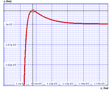
Fig. 3: Settling after a change of current
from 12uA to 10uA at t=11us
The simulation above shows the overshot
settling after a change of current from 12uA to 10uA at t=11us.
Id = K*SQR(Vg-Vth)
K is constant depending on the width, length,
oxide thickness and technology parameters such as bulk doping.
Vth is the threshold of the device and
Vg is the gate voltage actually applied.
Fig. 4: simple NMOS mirror
M1 simply creates a square root function
of Iin while M2 squares it again thus providing Iout being a replica of
Iin.
Since MOS transistors usually are designed
as small as possible short channel length is appreciated for cost reasons.
Since the electrical field of the drain acts as a gate the effective channel
length controlled by the gate gets shorter with increasing drain-source
volrage. Typical channel length modulations by the drain voltage are in
the range of 0.1um per Volt. In many MOS models this is reflected by the
parameter LAMBDA. So a typical output characteristic of a MOS mirror may
look as figue 5.
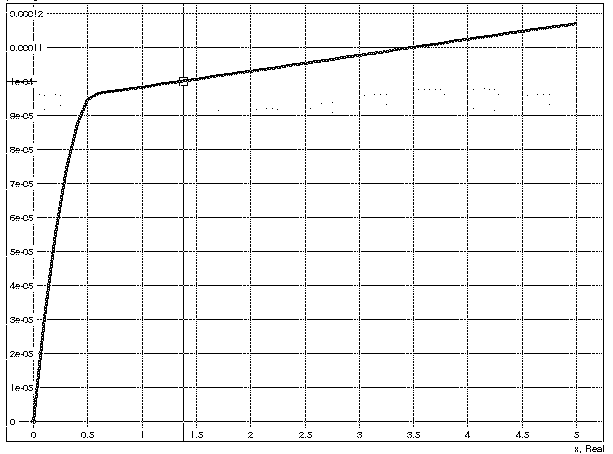
Fig. 5: Typical output characteristic
of an NMOS current mirror. X-axis: Vds, Y-axis: Id
To avoid the effect of channel length modulation keeping Vds of M2 constant using cascodes is the most common technolog.
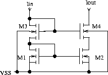
Fig. 6: NMOS mirror with cascode
In figure 6 M4 copies the drain voltage of M1 to the drain of M2 provided there is enough supply headroom available for M3 and M4.
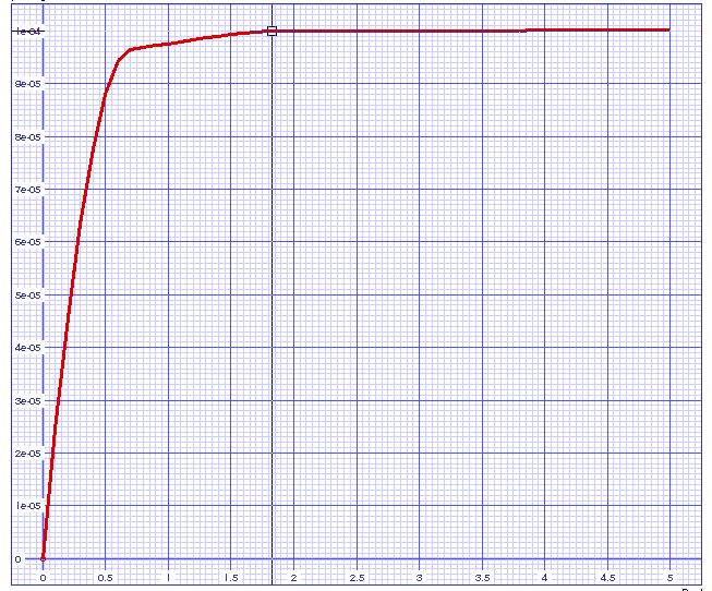
Fig. 7: Output characteristic of an NMOS mirror with cascode.
Be aware that the mirror works propperly
for drops (vds of M4) of more than twice the threshold! So this kinf of
mirror needs quite some headroom and is nott a good choice if low voltage
operation is desired.
In the circuit of figure 6 M2 operates
with a drain-source voltage of Vg, which is about 1.4V. Correct for high
precision, too much if we can accept a relative current error of (Vg-Vth)/Vearly.
The following mirror operates M2 at Vds=Vg-Vth.
This is exactly the transition between triode region and saturated region.of
operation.
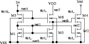
Fig. 8: Low drop cascode mirror still working in saturation
How does it work:
M1, M2, M5 work as usual with the same
current densities as before. So the voltage at net1 to be calculated as:
Id=K*SQR(Vg-Vth)
SQRT(Id/K) = Vg-Vth
lets call the effective gate voltage dVg
dVg = Vg-Vth
M3 operates at 4 times the current density of M1. So the voltage of net4 becomes:
V(net4) = V(net1) + Vth + SQRT(4*Id/K)
V(net4) = 2*Vth + dVg + 2*dVg
V(net4) = 2*Vth + 3*dVg
M6 operates at the same current density as M5. So the voltage at net6 becomes:
V(net6) = V(net4) - Vth -dVg
V(net6) = Vth + 2*dVg
Accordingly the voltage of net2 becomes:
V(net2) = V(net6) -Vth -dVg
V(net2) = dVg
So M2 operates exactly at the operating
point saturation starts at.
As soon at M4 reaches saturation too the
mirror operates with a high drain impedance. The voltage required at the
drain of M4 becomes:
Vout > 2*dVg
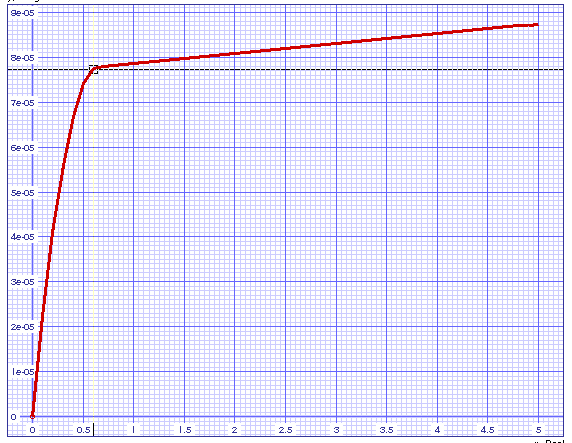
Fig. 9: Output characteristic of the low drop optimized mirror of figure 8
If we want to further reduce the operating
voltage of a current mirror we must knowingly operate M1 and M2 in triode
region. In this region the MOS transistors can simply be regarded as resistors.
So the mirror will work if the drain-source voltages of the reference element
(M1) and the output element are equal..
Figure 10 show a circuit achieving this
control of operating points.
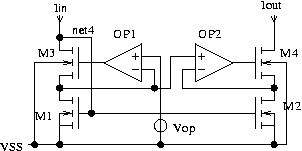
Fig. 10: Very low drop current mirror
Here Vop defines the operating point of
M1 and M2. OP1 and M3 regulate the drain voltage of M1 according to Vop.
OP2 and M4 establish a copy of the drain voltage of M1 at the drain of
M2.
In technologies featuring reproducable
resistors the circuit can be simplified:
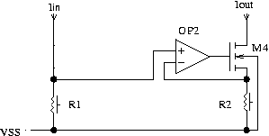
Fig. 11: Resistor coupled current mirror
So now we are back to one of the standard circuits used in discrete design.
References:
Most current mirrors using bipolar or MOS
components are described in detail in:
Gray, Meyer, 'Analysis and design of analog
integrated circuits', Wiley & Sons, 1977
Current mirrors using resistive characteristics
are described in:
Tieze, Schenk, 'Halbleiter Schaltungstechnik',
Springer, 1980