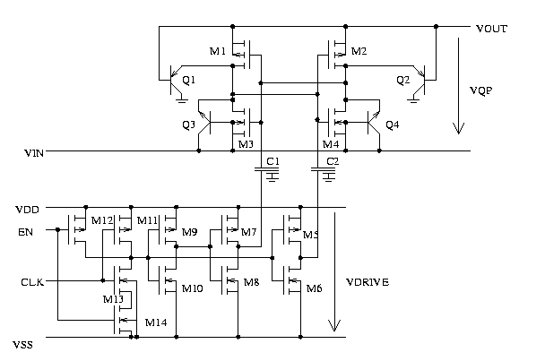
The circuit shows the intentional MOS transistors and the most important parasitic components.
Principal of operation:
The driver stages M7, M8,
M5, M6 are operating with inverse phase. The signal is capacitively coupled
to the CMOS latch M1, M2, M3, M4.
A rising edge at C1 turns
off M1 and pushes up the drain of M2. At the same time a falling edge at
C2 turns off M4 and turn on M2. C1 discharges into VOUT without a forward
voltage loss like in a bipolar rectifier. The successing falling edge at
C1 turns on M1. The simultaneous rising edge of C2 leads to a current flow
from C2 via M1 into Vout.
Charge lost in C1 during
the previous pulse will be recovered via M4 charging C1 up again.
Parasitc components:
The CMOS latch will not
operate propperly until VOUT is at least one MOS threshold higher than
VIN. So in the beginning charge pumping requires the bulk diodes of M1,
M3 and M2, M4. Due to the cact that most CMOS technologies have no burried
layer and sinkers like bipolar and power technologies these bulk diodes
incorporate bipolar parasitic transistors. The gains of these transistors
can reach values of 3 to 300 (depending on doping ratios and depth of the
wells)!
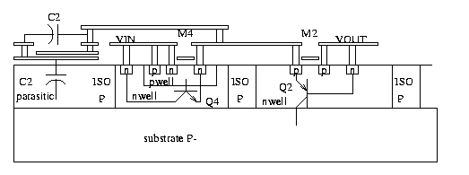
Special care must be taken
about the collector of Q3 and Q4. The nwell underneath the pwell of M3
and M4 must under no circumstances be connected to the output of the chargepump.
Otherwise the NPNs due to their high gain will prevent correct start up
of the circuit (during start up only a fraction of the charge pump current
comming out of the base of Q1 and Q2 is available while Q3 and Q4 have
the full pumping current available as base current!).
Even with no parasitic NPN
connected to VOUT during start up only a reduced output current (depending
on the gain of Q1 and Q2) is available.
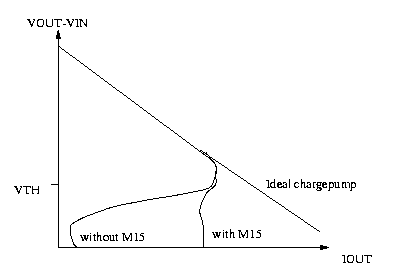
The above diagram shows the
load characteristic of an ideal charge pump, the chargepump discussed and
a chargepump disconnecting the load at low output voltage.
The capacitors C1 and C2
have parasitic capacities between the bottom plate and the silicon underneath.
Therefore the drivers M5 to M8 should be connected to the bottom plate
(unless a reduced output voltage is desired on purpose).
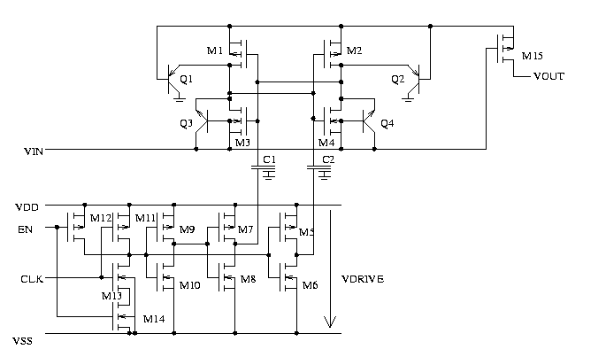
In
the improved chargepump M15 reduces the current supplied to the output
before Q1 and Q2 dump most of the current down into the substrate.
There
are alternative solutions described in literature such as pumping the bulks
of M1 and M2 with a second charge pump to prevent activation of Q1
and Q2. (See for instance Dragan Marksimovic, "Switched Capacitor DC-DC
Converters for Low Power On-Chip Applications", IEEE Journal of Solid State
Circuits 1999.)
VQP0 = VDRIVE
Since there always are some losses a slightly lower output voltage usually is measured. Typical practical implementations reach about:
VQP0 = 0.95*VDRIVE
Short
circuit output current can be calculate as follows:
Change
of charge of each capacitor in short circuit operation per clock period:
dQ = C*VDRIVE
So the short circuit current using 2 equal capacitors is:
I = 2*C*VDRIVE*fCLK
This way the output impedance can be calculated:
Rout
= VQP0 / (2*C*VDRIVE*fCLK)
Clocked
systems excite an analog simulator each time a clockedge takes place. Therefore
simulating a transistor level chargepump in a top level simulation leads
to excessive CPU time and unhandleable amounts of wafeform data.
To
overcome this problem two solutions are possible:
Ad (big analog part, small digital part) design usually are simulated with mixed mode approaches. The master simulator usually is an analog simulator. Here a behavioral model can be used.
Note that this model does
not use the CLK line. CLK only is a dummy pin needed to fit to the same
symbol as the original circuit. The simulation will not detect a problem
if the clock is not running! The presence of the appropriate clock must
be handchecked!
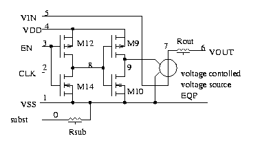
Pin subst usually is the
global node no 0 needed by simulators like SPICE. Since this is a global,
no pin is assigned in the symbol.
Some modern design libraries
have marker layers (for LVS) that allow connecting the substrate to VSS
(for simulation VSS becomes node 0 or is connected to node 0 in a higher
hierarchy level of the design). The wire subst is fully obsolete then.
aD (small
analog part, big digital part) designs usually are verified on top level
using a digital simulator such as verilog or VHDL. The chargepump then
must be represented by some digital
verilog code.
This approach does check
the clock line, but not the correctness of analog parameters (load behavior).