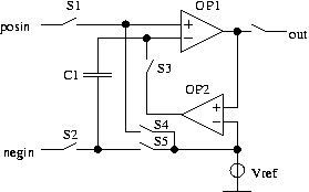
Fig. 1: Basic autozero topology with capacitor in the signal path
The
so called ping-pong topology allows operating the amplifier in open
loop configuration. This means the auto zero process can work even
while there is no feedback present. This typically is the case in
comparator applications.
A second advantage is the simplicity of the adjustment amplifier.
Usually this is a simple single stage amplifier with low gain
(sometimes even less than 0dB) and high bandwidth. The stability of the
feedback loop mainly is determined by main amplifier OP1.
A disadvantage of the ping pong topology is that the zero adjustment is performed in a different oprating point than that the amplifier is operating with. Depending on commom mode rejection there always remains a systematic error in the range of some 10uV.
To develop the
adjustment concept let us start with a single channel before adding the
second amplifier needed for a continuous signal.
Fig. 1: Basic autozero topology
with capacitor in the signal path
While
operating switches
S1, S2 and the switch to the output are closed and S3 to S5 are opened.
Assuming the charge stored in C1 is 0 the amplifier works as usual.
Adjustment:
To zero adjust the amplifier
S1, S2 are opened and S3 to S5 are closed. Assuming an ideal
(offsetless)
opamp OP1 the output voltage would be identical to Vref. Due to the
offset
voltage of OP1 OP2 will measure a deviation and charge C1 until Vout
approaches
Vref.
Due to the limited gain
of OP1 and OP2 the offset voltage will be reduced to about:
Voff_adjusted = Voffs / gain
Voff_adjusted
is the offset
voltage after adjustment. Voffs is the offset voltage of the
operational
amplifier OP1. gain is the product of the gain of OP1 and OP2.
In some cases for stability
reasons the gain of OP2 is choosen very low. In some cases a gain of
less
than 1 is choosen (OP2 then simply is a level shift with low gain).
To obtain high accuracy we need:
- low
initial offset Voffs
- high
gain of OP1 and OP2
- switches
with very litle clock feed through
- a large
capacitor C1 to attenuate remaining clock feed through
- very
low input bias current of OP1
- Vref
similar to the input voltage the amplifier is operated with
- a high
common mode rejection of OP1 (especially if Vref is not equal to the
typical
input voltage in operation)
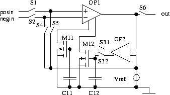
Fig 2: Auro zero op with
adjustment of the bias currents of the differential stage
Here OP2 is built fully differential. Through switches S31 and S32 the gates of M11 and M12 are charged until the input voltage of OP2 approaches 0V. Then the switches are opened. C11 and C12 hold the gate voltage and M11, M12 continue draining the adjustment current from the differential stage.
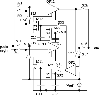
Fig. 3: Two amplifiers operating
intermittantly
In
this circuit OP1 simply
was duplicated. While OP11 gets adjusted (S16, S11, S12 are open) OP12
is connected (S26, S21, S22 closed) driving the output. When OP12 is
adjusted
OP11 is connected to the output.
If Vref is equal to the
signal voltage the settling time of the amplifiers can be reduced. An
alternative
solution is swapping the frequency compensation capacitors as well.
This
way the operational amplifier taking over already gets the last
operating
point of the amplifier active before as an initial state.
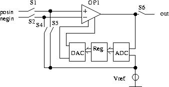
Fig. 4: Replacing OP2 of
fig. 2 by a digital control
This topology however adds some additional signals to the path: Since the correction is quantisized the offset either is overcompensated or undercompensated. The system will always move arround the correct value thus adding a carrier of half the sampling rate of the digital system. Assuming the amplifier acts more or less as an integrator most of the equations of a first order delta sigma converter apply. To distribute the unintentional carrier dithering with digital random noise could be used.
Once we regard OP1 as the dominant pole of the loop we can even reduce the ATD to a 1 bit converter, or more clear, a simple schmitt trigger. The register simply becomes an up/down counter.
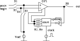
Fig. 5: Low cost auto zero
OP with digital storage.