Digital to Analog Conversion using R, 2R
Networks
(Published Jan. 2008)
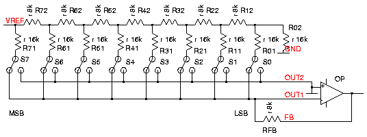
The following
figure shows the most common implementation of a digital to analog
converter using a R, 2R network. Since the amplifier is inverting the
output voltate is:
VFB = -VREF * DATA/2n
DATA is the content of the control word.
n is the power of 2 of the control word (8 in case of an 8 bit
converter)
Example D7=1, D6..D0=0 (S7 switched to the other position)
DATA = 27 = 128
n = 8
VOUT = -VREF * 128/256

Fig. 1: R2R DTA
Advantage of the
circuit
Compared to the
network using resistors with ratios
1:2:4:8... this network uses very similar resistor values. The
resistors R71, R61.. simply use the same geometry as the resistors R72,
R62.. except that two devices in series are used. Using the same
geometry for all components provides the best possible matching at
acceptable silicon real estate.
Implementations of this kind of network can be produced with acceptable
yield with up to 10 bit accuracy using standar silicon process.
For higher resolutions (up to about 12 bit) trimming of the resistors
is needed (at least on most standard silicon processes).
Special processes optimized for resistor matching (NiCr resistors etc)
combined with laser trimming can achieve resulutions of 14 bit and more.
Why is the OPAMP
needed?
One of the
limitations of the circuit is the error introduced by the switches
(Rdson). Of course it can be optimized adding 2 parallel closed dummy
switches in series with Rx2. Nevertheless the spread of the on
resistance of the switches remains as a source of errors.
The Rdson of the switches depends on the voltage between the control
gate and the channel. To always achieve the same contribution of the
switch every switch must be connected to the same (or almost the same)
potential. Using the circuit shown above the switch always is either
connected to ground or to virtual ground at the negative input of the
amplifier (assuming the gain of the amplifier is high enough).
Other implementation using floating switches each having an individual
(different from the other switches because channel potentials are not
similar to ground) voltages between the gate and the channel lead to
higher errors caused by the Rdson of the switches.
Literature:
There is a lot of
more detailed literature available. Here are only a few examples:
Intersil Data sheet AD7523, about 1985
Geiger, Allen, Strader, 'VLSI Design Techniques for Analog and Digital
Circuits', McGraw Hill, 1990
National Semiconductor Application Note AN-284, 'Single Supply
Applications of CMOS MICRODACs', 2003
